Staera Raises $4.6M to Industrialize Lightwire
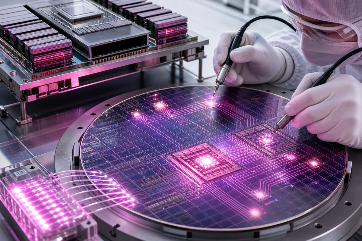
Staera Semiconductor, formerly NSC, announces Lightwire, an optical interconnect manufactured directly within the chips. The startup has secured $4.6 million in pre-seed funding to transition from the lab to product, aiming for a launch in 2030 with claimed energy and throughput performance significantly superior to current solutions.
Lightwire aims for less than 50 W for 24 To/s and over 600 links per mm
According to Staera, transferring 24 terabytes per second with Lightwire would require less than 50 watts, while co-packaged optics would need nearly a kilowatt. The company reports data rates of 4 to 8 Gbps per link, with a density exceeding 600 links per millimeter on the chip edge. The system targets a consumption of less than 0.2 pJ/bit, compared to 5 pJ/bit for co-packaged optics, and claims performance exceeding one hundred times that of electrical links over distances ranging from millimeters to meters. The distance covered would exceed 50 mm, while a UCIe-A die-to-die link only spans 2 mm. An HBM based on Lightwire would aim for a throughput greater than 24 TB/s, whereas a current HBM4 stack reaches 2.8 TB/s. Lightwire is also described as using less than one-tenth of the energy consumed by the best optical links available and integrates into the bridge chip or interposer already connecting processors and memory, ensuring compatibility with existing packaging solutions. The device is designed to operate in parallel with copper.
A $4.6 million pre-seed round to move to product and target 2030
Staera has raised $4.6 million in pre-seed funding, led by Openspace Capital with participation from SGInnovate, Black Kite Capital, 28 Holdings, In Group, and Decimus Technologies. According to the company, this funding marks the transition from research to commercial product. The funds are intended to advance the technology, expand the team, and strengthen relationships with customers and supply chain partners. The company aims for a commercial launch in 2030. Andrew Kim believes this funding allows Lightwire to move from the lab to customers, and that the name change to Staera accompanies this milestone.
Le brief IA que les pros lisent chaque soir
Les 7 actus IA du jour, décryptées en 5 min. Gratuit.
Inclus dès l'inscription : notre sélection des meilleurs guides & comparatifs IA.
Choisissez votre rythme
Gratuit · Pas de spam · Désabonnement en 1 clic
Manufacturing in existing foundries and full integration on silicon
Staera combines standard silicon CMOS processes, GaN, and waveguide layers on a single wafer. The company specifies that it produces the light source as well as all components of the optical link directly within commercial wafers, describing Lightwire as the first fully integrated optical interconnect on the chip. These links are intended to be manufactured in already operational foundries and, according to Staera, do not involve increased size, heat dissipation, or excessive energy consumption. The company claims to have integrated GaN LEDs in commercial foundries since 2016, with current yields of 98 to 99%. Its LED-based optical interconnect, produced in a single chip, aims to transport data via light rather than electricity, with the density necessary for paths ranging from a few millimeters to several meters without declared compromises.
Energy context, adoption threshold, and market signals
The International Energy Agency estimates that electricity consumption in data centers could more than double, from nearly 415 TWh in 2024 to about 945 TWh in 2030, while copper requires more energy to carry more data over longer distances. Nvidia, which indicated in 2025 that it would stick with copper for as long as possible, now anticipates a combination of copper and optics, a configuration for which Lightwire is designed. On the investor side, Hian Goh of Openspace Capital describes the challenge addressed by Staera as the movement of massive volumes of data between chips without a correlated increase in energy, heat, and complexity, and sees direct silicon integration as a pathway to faster, more efficient, and scalable AI systems. He explains his support for the startup due to its technology, team, and potential to define a new category. Staera received recognition in May 2026, winning the 3rd ECTC startup competition at the IEEE ECTC conference and securing a finalist position in the 2026 Lam Capital competition by Lam Research in Fremont, California. Andrew Kim, CEO of Staera, asserts that the bottleneck lies in data movement, that copper's performance declines over distances on the order of millimeters to meters, and that added optics increase consumption and complexity; he emphasizes the complete integration of the link into the chip and the announced smaller, cooler, and faster connections with each generation.
Brief IA — L'actualité IA en français
L'essentiel de l'actualité de l'intelligence artificielle, décrypté et expliqué chaque jour.